Texas Instruments UCC23113 Isolated Gate Driver
Texas Instruments UCC23113 Isolated Gate Driver is an opto-compatible, single-channel, isolated gate driver for IGBTs, MOSFETs, and SiC MOSFETs. The device has a 5A source, 5A sink peak output current, and 1.5kV DC functional isolation. The high supply voltage range of 30V allows the use of bipolar supplies to drive IGBTs and SiC power FETs effectively. The UCC23113 can drive both low-side and high-side power FETs.
Key features and characteristics bring significant performance and reliability upgrades over standard opto-coupler-based gate drivers while maintaining pin-to-pin compatibility in schematic and layout design. Performance highlights include high common-mode transient immunity (CMTI), small pulse width distortion, and low propagation delay. A tight process control results in a small part-to-part skew. The input stage is an emulated diode (e-diode), which means excellent aging characteristics and long-term reliability compared to traditional LEDs found in optocoupler gate drivers. The device is offered in a stretched SO6 package with > 8.5mm clearance and creepage and a mold compound from material group I with a comparative tracking index (CTI) > 600V.
The high performance and reliability of the Texas Instruments UCC23113 make it ideal for use in all types of solar inverters, motor drives, appliances, and industrial power supplies. The higher operating temperature of the device opens up opportunities for applications not previously able to be supported by traditional optocouplers.
FEATURES
- 1.5kV DC single channel isolated gate driver with opto-compatible input
- Pin-to-pin, drop-in upgrade for optoisolated gate drivers
- 5A source/5A sink, peak output current
- Maximum 30V output driver supply voltage
- 12V VDD undervoltage lockout
- Rail-to-rail output
- 105ns (maximum) propagation delay
- 25ns (maximum) part-to-part delay matching
- 35ns (maximum) pulse width distortion
- 100kV/µs (minimum) common-mode transient immunity (CMTI)
- 5V reverse polarity voltage handling capability on input stage supporting interlock
- Stretched SO-6 package with > 8.5mm creepage and clearance
- Operating junction temperature, TJ of -40°C to +150°C
APPLICATIONS
- Industrial motor-control drives
- Solar inverters
- Industrial power supplies, UPS
- Induction heating
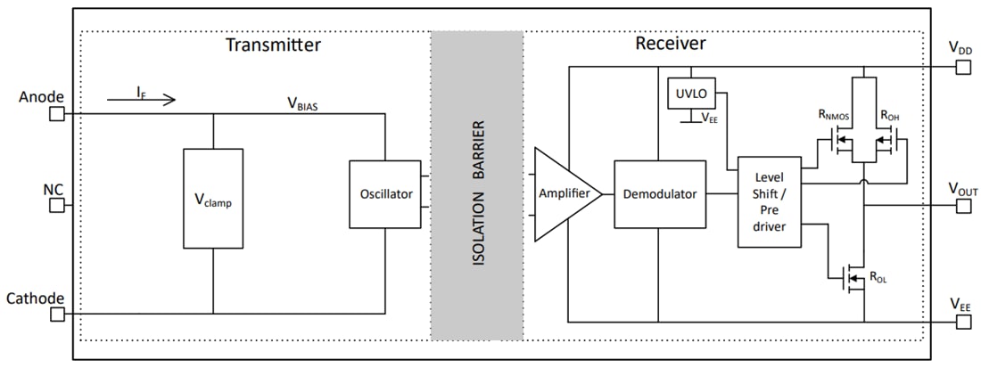
FUNCTIONAL BLOCK DIAGRAM


